Emerging Device Physics Lab. @ EWHA
Research Facilities
Atomic force microscopy systems (Park Systems, XE-100 & NX10)
- Glove box to control the ambient
- Sample temperature stage w/ a Peltier device
- PCB board for simultaneous electrical characterizations
- LED light sources w/ polarizers
Micro-fabrication equipment in a clean room
- Mask aligner
- Wet station
- Optical microscope (Nikon)
- Surface profilometer (Dektak)
- Reactive ion etcher (SBT RIE2000)
- Electron-beam evaporator (Telemark)
- RF magnetron sputterer
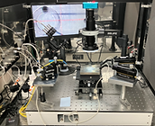
Dry transfer set-ups for 2D materials


Probe station w/ a hot chuck (Instek)
Variable-temperature vacuum probe station (Janis ST-500)
- Semiconductor characterization system (Keithley 4200)
- Digital oscilloscope (Tektronix DPO4104)
- Sourcemeter (Keithley 2400)
Micro-Raman/PL system (Nanobase)
- 532 and 633 nm lasers (Cobolt)
- Scanning photocurrent mapping
Angle-resolved reflectance measurement setup
Wire bonder (Westbond)
Workstation for FDTD simulations (Lumerical)